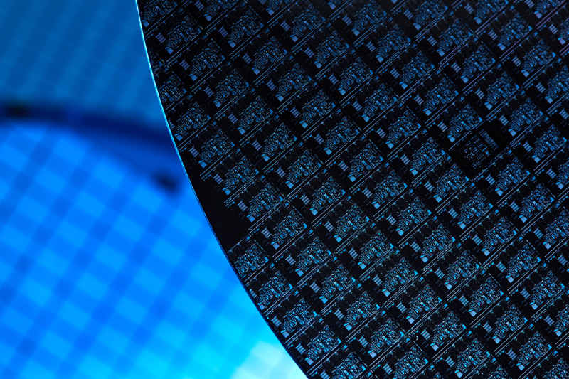
Physical Design (PD)
TechM Semicon emerged as a world class expertise to provide best chip design solution for its customers with its focused and efficient specialized team in backend physical design with a legacy of 40+ tape-outs in technology nodes varying from180 nm to 10nm.
Our well-trained engineers in backend design are expertise with all the popular industry standard tool flows and have experience working with leading fab houses.
We excel at delivering perfect product designs at fast turnaround with our well-defined and customizable execution and sign-off processes.
Our services include
IP/Block Hardening:
Expertise in mixed signal and digital IP hardening. Work experience on high speed interface IPs such as DDR, Serdes
Full Chip or Block Level Implementation:
Expertise in end to end flow from RTL/netlist to GDSII. Design planning, full chip level floorplan, bump planning, RDL implementation, timing budgeting, power planning, PnR

Expertise
Technology nodes
Worked on all latest nodes 14nm, 10nm and 7nm.
Design Complexity
1.5 million gates to 10million gates with multiple clock domains and power domains.
Low Power
Multi power domains upto 6 domains, expertise in designing power intent, low power checks, design sanity.
Fab Houses
Team has experience in working with all leading fab houses.
Tools
Worked with all popular industry standard tool flows like Synopsys, Cadence, Magma, Mentor, Apache.
DFT
We have expert management to oversee project progress, methodology, checklists and regular reviews to ensure predictable results and schedule. We offer complete physical implementation services which includes Synthesis, DFT, Floor planning, IO placement, block placement, Power planning, CTS, Place & Route, Physical verification ATPG and STA signoff.
